v3Di V3D Interaction
The Technology Leader in Volumetric 3D Display

PhotoElectroforming (MEMS fabrication)
Field: Manufacturing/MEMS
Topic: Photo-Electroforming
(Che-Chih Tsao's MIT Ph.D. / Post Doctorate work)
Summary
Photo-electroforming builds parts by an additive process which defines geometry by depositing powder in layers and creating regions of selective conductivity by laser-enhanced electroless plating. The conductive region is then joined by a second plating to form an integral part. The unmetallized portion is removed by selective etching in one step after all layers are defined and joined. Single-layer and two-layer stand-alone parts made of nickel/silicon carbide composites of overall size 75-100 μm and feature size 25μm were created. Writing speeds of up to 24 cm/s and in-plane resolution of 15 μm were demonstrated. A continuous process using a flow through bed with continuous deposition of 5 μm nickel power and selective joining by laser induced nickel plating was also studied.
Single layer and double layer SiC/Nickel parts created by layer-by-layer process.
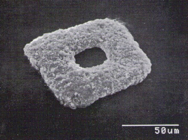
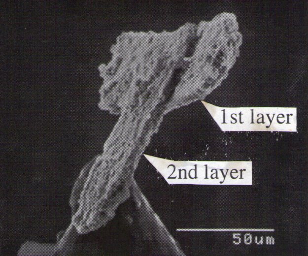
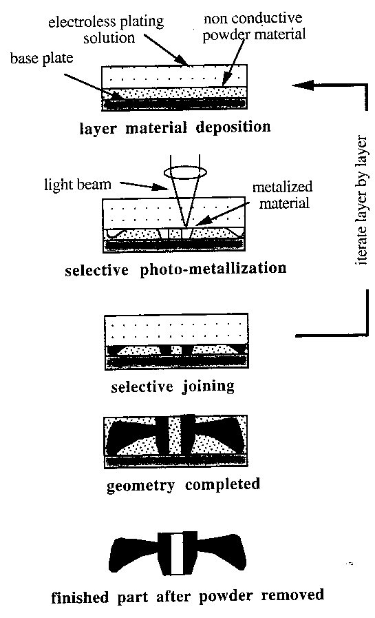
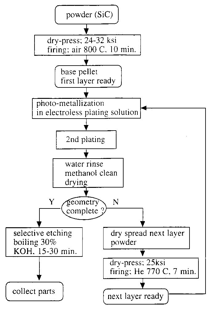
(Left) General Photo-Electroforming conept. (Right) Layer-by-layer process using silicon carbide powerder and nickel plating as an example.
Major innovations/contributions:
-- A layer by layer micro-fabrication process for making parts of metal-ceramic materials.
-- Laser-induced plating rates were found to be due to elevated substrate temperatures under the laser spot and enhanced mass transfer due to pumping by the hydrogen bubbles resulting from the plating reaction.
-- Ibl and Venczel’s bubble displacement model for hydrogen generating electrode was applied, for the first time, to study laser enhanced electroless plating A continuous process for making all-metal part (nickel) by laser induced electroless plating.
-- Crossed dual beam arrangement for confined heating zone to prevent high rate over deposition in undesired direction.
Patent / Publication:
E.M. Sachs and C. Tsao, US Pat. No. 5,512,162, "Method and Apparatus for Photo-Forming Small Shaped Metal Articles from Porous Precursors and Articles Fabricated according to the Method"
C. Tsao and E.M. Sachs, "Photo-Electroforming: 3-D Geometry and Materials Flexibility in a MEMS Fabrication Process", Journal of MicroElectroMechanical Systems, v8 n2 p161-171